

// Mission-Critical Production //
High-Precision SMT & PCBA Product Offerings
Explore our industrial turnkey assemblies engineered to resolve component life-cycle bottlenecks, legacy microelectronics shortages, and next-generation smart computing demands.

Custom Shenzhen SMT PCBA for Smart Products
Explore Specification
ODM One-stop PCBA & PCB Assembly
Explore Specification
OEM Smart Bracelet Micro PCBA
Explore Specification
Custom PCBA from Gerber & BOM Files
Explore Specification
High-Power PCBA Assembly with DIP Wave
Explore Specification
Custom PCBA for IoT Control Systems
Explore Specification
Professional SMT PCBA Turnkey Service
Explore Specification
// Industry Whitepaper & Strategic Insights //
Commercial Realities of End-Of-Life (EOL) Electronics Assembly
Managing the lifecycle curve of printed circuit board assemblies requires moving past transactional manufacturing to continuous reverse engineering, component sustaining, and legacy redesign architectures.
In modern industrial electronics, aerospace, healthcare, and telecommunication infrastructure, the lifecycle mismatch between semiconductor manufacturing roadmaps and operational product service lifetimes has become a critical operational vulnerability. Silicon vendors routinely issue Product Discontinuation Notices (PDN) and End-Of-Life announcements within 3 to 7 years. Conversely, mission-critical assets—such as medical diagnostic suites, power grid relays, rolling-stock railway control electronics, and automated factories—are expected to deliver reliable continuous performance across a 15- to 30-year operational horizon.
As a seasoned OEM End-Of-Life PCBA Solution Manufacturer & Supplier based in Shenzhen, Aozite delivers closed-loop manufacturing frameworks specifically architected to prevent line-down catastrophes caused by EOL silicon. Our engineering paradigm bridges the chasm between obsolete bill-of-materials (BOM) components and active assembly lines without necessitating exorbitant recertification investments or complete architectural overhauls.
Macro Market Dynamics: The Rising Imperative for EOL Assembly Solutions
The global electronics sector faces structural changes driven by geopolitical realignments, the rapid obsolescence cycles of AI-optimized consumer chips, and fab capacity prioritization toward deep-submicron nodes (<7nm). Consequently, trailing-edge nodes (such as 90nm to 180nm)—the fundamental foundation for high-voltage industrial microcontrollers, CAN transceivers, op-amps, and motor drivers—face frequent fab consolidation, discontinued wafer runs, and sudden lead time shocks.
Node Abandonment Pressure
Global semiconductor foundries continue to repurpose trailing-edge production lines to automotive-spec silicon or high-margin automotive PMICs, systematically abandoning low-margin legacy microcontroller packages.
- Sudden Last-Time Buy (LTB) notices
- Soaring minimum order quantities (MOQs)
- Package phase-outs (e.g., PLCC, DIP, TSOP)
Counterfeit Vulnerability & Risk
Desperation in the open gray market exposes OEMs to high counterfeit risks. Gray-market microchips frequently exhibit re-topped packages, non-functional internal dies, sandblasted date codes, and prior thermal stress.
- Rigorous X-ray and decapsulation audits
- Solderability testing for aged leads
- Destructive physical analysis (DPA)
Certification & Compliance Drag
Complete product redesign triggers protracted and expensive compliance re-validations (CE, UL, FDA Class II/III, ISO 13485, ATEX). Sustaining existing PCBA form-factor and functional integrity remains the most cost-effective path.
- Avoidance of complete system recertification
- Form-Fit-Function (FFF) replacement
- Seamless drop-in mechanical drop compatibility
// Methodological Framework //
End-to-End EOL PCBA Sustaining Roadmap
A structured, multi-tier engineering approach to maintaining legacy assemblies, extending revenue horizons, and eliminating supply disruptions across four specialized execution phases.
PHASE 01 // AUDIT
BOM Health & EOL Vulnerability Scoring
Silicon lifecycle scrub across global databases (IHS Markit, SiliconExpert). Identification of single-source silicon, immediate LTB requirements, and impending component obsolescence risks.
PHASE 02 // SOURCING
Authorized Global Sourcing & Traceability
Procurement through franchise tier-1 networks, manufacturer-authorized surplus channels, and nitrogen-purged moisture-controlled warehousing for multi-year strategic stock reserves.
PHASE 03 // REDESIGN
FFF Redesign & Interposer Engineering
Form-Fit-Function drop-in re-engineering. PCB re-layout using active QFN/BGA silicon, or micro-interposer daughterboards that interface seamlessly with obsolete footprint pinouts.
PHASE 04 // VALIDATION
Automated FCT & Reliability Verification
Thermal cycling, boundary scan, custom FCT test fixture development, and firmware patch validation ensuring electrical and temporal parity with legacy operations.
Engineering Beyond Obsolescence: Form-Fit-Function (FFF) and Daughterboard Emulation
When silicon reaches absolute terminal discontinuation and stock runs completely dry, modernizing without altering the outer enclosure, backplane harness, or system software becomes paramount. Aozite's specialized engineering unit provides Daughterboard/Interposer Sub-Module Assembly. By redesigning an active, miniaturized micro-controller or FPGA core onto a miniature HDI rigid-flex or high-density FR4 carrier with perimeter castellations, we replicate obsolete pin-grid-arrays (PGA), quad-flat packages (QFP), or dual in-line packages (DIP). This delivers zero firmware rewriting and instantaneous line revival.
// Mission-Critical Use Cases //
Macro Industry Applications & Targeted Solutions
Discover how our Shenzhen manufacturing base safeguards mission-critical systems across core high-reliability industrial segments.
Industrial Automation & Robotics
Continuous Sustaining for PLCs, Motion Controllers & Drives
Factory automation lines rely on legacy fieldbus communication standards (Modbus RTU, Profibus, CANopen) integrated into heavy-duty SMT and DIP assemblies. We manufacture replacement and sustained PCBA runs for factory machinery operating continuously over decades, mitigating component dry-outs and obsolescence.
- High-reliability conformal coating (silicone, acrylic, polyurethane) against chemical mist
- Wave and selective soldering for legacy high-current power connectors
- In-house burn-in aging chambers for industrial operating temperature bounds (-40°C to +85°C)
Medical Diagnostics & Healthcare
Regulatory-Compliant Sustained Medical PCBA Manufacturing
Changing an integrated circuit on an FDA Class II or Class III medical device often demands full clinical re-audits costing millions. Aozite supports med-tech OEMs with strict lot-traceability, controlled clean-room assembly, and component preservation techniques to satisfy IPC Class 3 quality thresholds throughout extended product cycles.
- 100% automated optical inspection (AOI) + 3D X-Ray (AXI) for zero voiding
- Full traceability records maintained for 10+ years per device lot
- Class 10,000 ESD-protected assembly spaces with stringent climate monitoring

Automotive & Transportation
Harsh Environment PCBA for Heavy Vehicles & EV Subsystems
Transportation and smart-mobility infrastructure cannot afford sudden supply halts. Our factory manufactures automotive-grade sub-assemblies for battery management systems (BMS), telemetry modules, and in-cabin body control modules (BCM) engineered to withstand ongoing vibrational harmonics and thermal shock.
- IPC-A-610 Class 3 workmanship and J-STD-001 soldering standards
- Component moisture baking and re-balling protocols in controlled dry cabinets
- Electrochemical migration and ionic contamination testing
// Technological Roadmap //
Future Outlook: AI, Smart Warehousing & Re-Engineering Automation
The convergence of predictive AI algorithms and smart agile surface-mount manufacturing is transforming how global OEM enterprises resolve printed circuit board obsolescence.
Historically, solving an End-Of-Life microelectronics bottleneck relied on fragmented manual brokers, static spreadsheets, and reactive fire-fighting. Today, leading manufacturers leverage Algorithmic Lifecycle Forecasting to aggregate foundry wafer starts, lead-time movements, and end-of-life notices years ahead of physical material shortages.
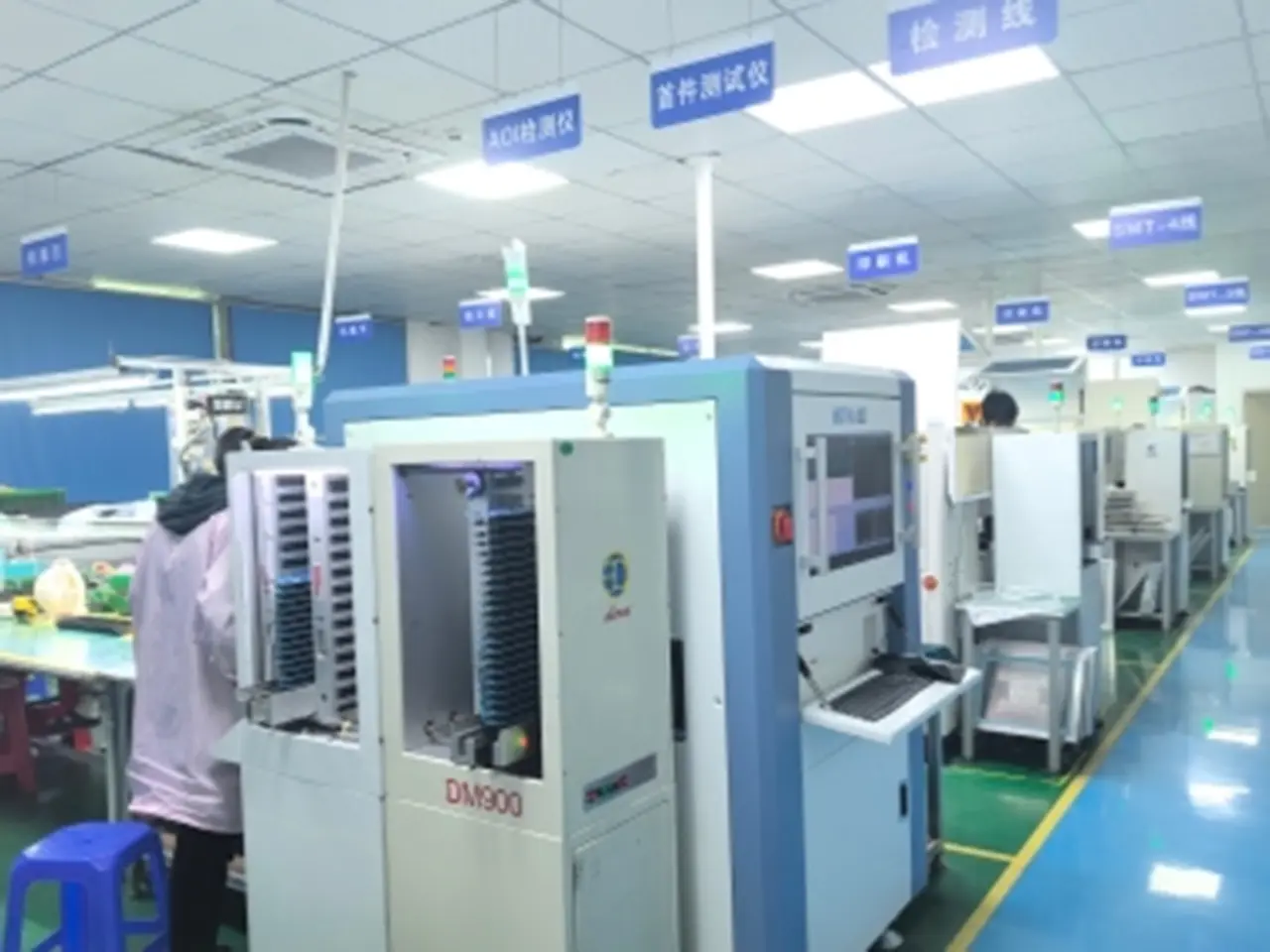
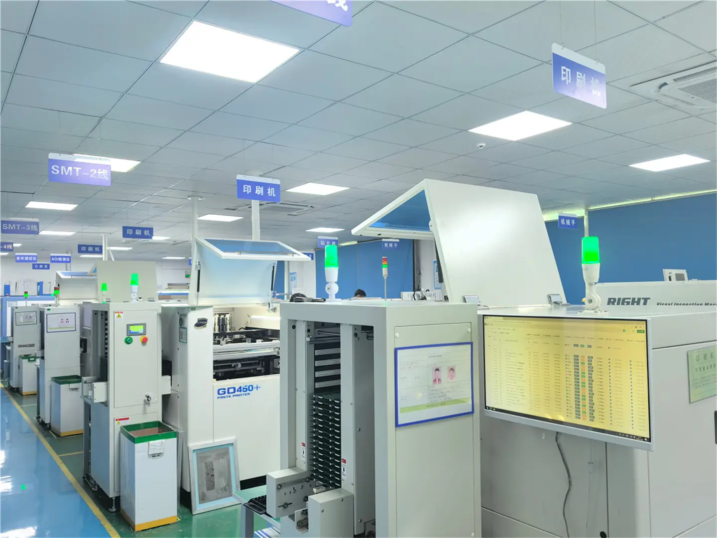
Shenzhen Aozite Technology continues to integrate smart manufacturing capabilities into daily production workflows. Located directly within the Pearl River Delta electronics cluster, our facility pairs automated pick-and-place precision (handling passives down to 01005 and 0.3mm fine-pitch BGAs) with automated component baking, laser marking, and advanced automated rework fixtures. Whether an OEM requires short-run bridge manufacturing during silicon transitions or permanent 15-year lifecycle preservation, modern turnkey operations guarantee seamless mechanical continuity, firmware compatibility, and stable cost structures.
AI Predictive Sourcing
Machine learning scanners evaluate enterprise BOMs in real-time, monitoring obsolescence velocity and issuing early warning flags before public PDN release.
Hermetic Micro-Storage
Active nitrogen purge chambers and continuous desiccant monitoring safeguard legacy components for up to 10 years without lead oxidization or MSD degradation.
Rapid In-Circuit Emulation
FPGA and system-on-module (SoM) synthesis capable of hardware-emulating retired 8-bit, 16-bit, and legacy DSP architectures on identical pin definitions.
Zero-Defect Reflow Profiles
Thermodynamic reflow profiling customized for mixed-alloy soldering—allowing leaded legacy components and modern RoHS lead-free matrices to fuse without thermal fatigue.
// Technical Answers //
End-Of-Life PCBA Solutions: Comprehensive FAQ
Authoritative technical guidance compiled by senior SMT manufacturing directors and supply chain engineers for procurement officers and engineering leaders.
What exactly is an End-Of-Life (EOL) PCBA Solution?
An End-Of-Life (EOL) PCBA Solution is a specialized engineering and electronics manufacturing service that sustains, repairs, redesigns, or continues production of circuit board assemblies whose critical components (such as MCUs, ASICs, power regulators, or passive arrays) have been discontinued by original component manufacturers. It combines global lifecycle sourcing, Form-Fit-Function (FFF) board redesign, daughterboard interposers, reverse engineering, and specialized test-fixture fabrication to ensure the OEM's end-product continues shipping without system redesigns or recertification penalties.
How do you verify the authenticity of obsolete or hard-to-find components?
Our quality control laboratory applies rigorous multi-stage component testing conforming to IDEA-STD-1010 and AS6081 standards. Incoming legacy silicon undergoes:
- Visual Microscopic Inspection: Verifying lead finish, indentation markings, and mold markings for evidence of sanding or re-topping.
- Acetone & Chemical Swab Testing: Checking package coating integrity against remarking solvents.
- 3D Real-Time X-Ray (AXI): Examining internal bond wire integrity, die orientation, and leadframe consistency against known golden samples.
- Decapsulation & Die Inspection: Chemically opening sample packages to verify the original silicon manufacturer logo and die mask rev codes.
- Solderability & Electrical Testing: Ensuring aged leads wet properly without requiring excessive reflow temperatures that jeopardize component lifespan.
What is a Form-Fit-Function (FFF) Redesign, and when is it necessary?
An FFF redesign creates a modified circuit board assembly that matches the predecessor's exact physical footprint (Form), mechanical mounting and connectors (Fit), and electrical and firmware performance (Function). It becomes necessary when an essential IC is unavailable globally, and Last-Time Buy inventory is exhausted. By replacing discontinued silicon with active chips through subtle PCB layout adjustments or miniature daughterboard adaptors, OEMs avoid recertifying the broader end-equipment (e.g., medical carts, industrial cabinet controllers, rail traction boxes).
Can you handle mixed soldering processes (Leaded Legacy vs. Lead-Free RoHS)?
Yes. Many legacy military, aerospace, and high-reliability industrial assemblies require tin-lead (Sn63Pb37) solder to prevent tin whisker formation and endure severe thermal shock. However, modern replacement passives are strictly lead-free (RoHS). Our 8 SMT lines feature multi-zone nitrogen-reflow ovens with independently monitored thermal zones, enabling us to configure tight reflow profiles that successfully solder backward-compatible mixed metallurgies without cold solder joints or component overheating.
How does Aozite manage long-term strategic buffer inventory?
For OEM partners requiring sustained PCBA production over 5 to 10 years, we provide turnkey strategic safety stock warehousing. Procured legacy silicon is registered with complete lot documentation, vacuum-sealed with humidity indicator cards (HIC), and stored in continuous nitrogen-purged dry cabinets maintained below 5% relative humidity (RH). This eliminates oxidation and moisture-sensitive device (MSD) popcorning during future production runs.
What data package is required to initiate an EOL PCBA sustaining project?
To evaluate an EOL project, please provide:
- Complete Bill of Materials (BOM): Detailing manufacturer part numbers (MPN), approved alternate vendors, and designators.
- CAD/Gerber Data: RS-274X or ODB++ fabrication and assembly files.
- Pick and Place / Centroid Data: Component placement coordinates.
- Firmware & Test Procedures: Complete Functional Circuit Test (FCT) guidelines, pinout voltages, and acceptable tolerances to validate drop-in parity.
// Scalable Production Capacity //
End-to-End Turnkey Assemblies & Specialized Processing
Seamlessly scale from rapid prototyping to sustained high-volume manufacturing. Select your required circuit board assembly architecture below.

Industrial Control PCBA Processing Service
View Manufacturing Specs
ODM Earphone Panel Ultra-Compact PCBA
View Manufacturing Specs
Consumer Electronics PCBA Line Build
View Manufacturing Specs
Smart Home Control Module PCBA
View Manufacturing Specs
Full Turnkey PCBA Box-Build Solutions
View Manufacturing Specs
Wearable High-Density Interconnect PCBA
View Manufacturing Specs
Gerber-to-Board Custom Assembly
View Manufacturing Specs
Heavy-Copper Power Conversion PCBA
View Manufacturing SpecsIPC-A-610 Class 2 & 3
Standard & Mission-Critical Builds
100% In-Line 3D SPI & AOI
Paste Height & Joint Inspection
Advanced BGA X-Ray (AXI)
Void Percentage Audit <10%
ESD Controlled (ANSI/ESD S20.20)
Complete EPA Protected Facility