
High-Reliability PCBA Manufacturing Solutions
Explore our core engineering builds engineered for demanding operational regimes, thermal endurance, and rapid turnaround verification.

China Custom PCBA Production from Gerber & BOM Files Service, Factories
Explore Product
High-Quality OEM ODM PCBA for All Electronic Products Service, Factory
Explore Product
Custom High-quality PCBA Assembly for IoT Control Boards Supplier, Factory
Explore Product
Custom Shenzhen SMT PCBA for Smart Product Manufacturing Service, Factory
Explore Product
OEM Professional SMT PCBA Production for Electronics Manufacturers, Supplier
Explore Product
High-Quality Industrial Control PCBA Assembly & Processing Service Supplier, Suppliers
Explore Product
ODM Earphone Panel PCBA OEM ODM Service Supplier, Factory
Explore Product
OEM Smart Bracelet PCBA OEM Manufacturing Factories, Factory
Explore ProductThermal Cycling Stress & PCBA Solder Joint Integrity
Understanding mechanical fatigue, intermetallic compound growth, and failure mechanics in modern electronics operating under harsh cyclic thermal loads.
CTE Mismatch Mitigation
Disparities in Coefficient of Thermal Expansion (CTE) between silicon dice, FR4/polyimide laminates, and solder alloys create severe shear stress during thermal fluctuation. Controlled DFM profile balancing protects joints.
- Substrate CTE stabilization (14-17 ppm/°C)
- Underfill dispensing for flip-chip & fine-pitch BGA
- Solder pad geometry optimization per IPC-7351B
Intermetallic Compound (IMC)
Prolonged dwell at elevated temperatures accelerates Cu6Sn5 and Cu3Sn compound formation at the boundary layer. Excess IMC layer thickness (>4µm) induces brittle interfacial fracturing under cyclic shear.
- Accurate 10-zone nitrogen reflow profiling
- Strict control of peak dwell time (TAL 45-65s)
- Sn-Ag-Cu (SAC305) & low-void micro-alloying
Thermal Fatigue Testing Protocols
Our in-house and partnered validation regimes adhere strictly to global stress screening standards, identifying early latent defects, barrel cracking, and pad lifting before field deployment.
- JESD22-A104: -40°C to +125°C thermal cycling
- IPC-9701: Performance qualification of solder joints
- Continuous daisy-chain in-situ resistance monitoring
Global Enterprise Sourcing Demands for Critical Assemblies
Original Equipment Manufacturers across North America, Europe, and Asia-Pacific require verifiable process control metrics rather than standard commercial warranties.
| Evaluation Vector | Commercial Grade PCBA | Thermal Cycling Qualified PCBA (Aozite) | Impact on Field Lifespan |
|---|---|---|---|
| Laminate Specification | Standard FR-4 (Tg 130-140°C, Td 300°C) | High-Tg FR-4 / Polyimide (Tg ≥ 170-180°C, Td ≥ 340°C) | Prevents z-axis trace stretching and via rupture during thermal shifts. |
| Solder Paste Voiding | IPC Class 2 (≤ 25% voiding under BGA) | IPC Class 3 + Vacuum Reflow (≤ 10-12% voiding) | Eliminates hotspot entrapment and premature solder ball shear collapse. |
| Inspection Regimes | Sample AOI, manual visual sampling | 100% 3D SPI + 100% Inline 3D AOI + Dual-Angle 3D AXI | Detects hidden solder bridging, wetting lift, and internal micro-cracks. |
| Traceability Level | Batch / Reel level lot tracking | Unit-level 2D DataMatrix (Component reel, reflow log, test record) | Enables single-board recall isolation without broad fleet grounding. |
| Post-Assembly Coating | None or localized spot manual coating | Automated Selective Conformal Coating (Acrylic/Silicone/PU) | Protects against condensation, moisture condensation, and creep corrosion. |
Shenzhen SMT Infrastructure: Resilience & Velocity
Combining the dense component supply chain of Greater Bay Area with intelligent SMT manufacturing lines for rapid prototyping and mass-scale volume execution.
Sub-4hr Kitting Proximity
Direct physical access to original chip makers and top-tier authorized distributors enables same-day BOM allocation and rapid lead-time recovery.
Automated MES Line Control
Centralized Manufacturing Execution System (MES) links solder stencil printing, Yamaha/Panasonic placement, and thermal profile telemetry.
ESD & Cleanroom Control
Class 100,000 cleanroom environments, active static dissipative flooring, and continuous relative humidity monitoring suppress latent component fatigue.
Rapid Line Changeovers
Intelligent feeder docks and automated optical calibration enable smooth transition between rapid NPI pilot runs and multi-thousand unit mass production.
Where Thermal Cycling Reliability Directly Governs Uptime
Real-world industrial installations require PCBA hardware to endure rapid cyclic temperature transitions without signal loss or physical joint degradation.
Automotive & EV Powertrain
Under-the-hood and inverter electronics encounter temperature swings from -40°C winter cold soaks to +135°C motor drive operations. We deploy high-temperature solders and precision conformal coatings to prevent cracking.
- Battery Management Systems (BMS)
- On-Board Charger (OBC) modules
- DC-DC converters & traction drives
Outdoor Telecommunications & Edge AI
Pole-mounted 5G remote radio heads and trackside IoT compute nodes experience severe diurnal thermal swings. Thermal modeling and structural heat sinking are integrated during initial DFM review.
- 5G NR active antenna arrays
- Ruggedized roadside IoT gateways
- Remote satellite transceiver arrays
Industrial Automation & Smart Energy
Variable frequency drives, smart solar inverters, and oilfield sensors withstand extreme continuous heat dissipation alongside sharp cyclic load spikes, demanding void-free soldering surfaces.
- Solar microinverters & MPPT controllers
- Factory PLC and robotics controllers
- High-power industrial switching gear
Multi-Stage Verification Process For High-Reliability PCBA
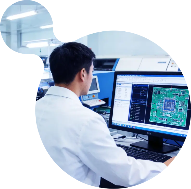
Zero-defect manufacturing requires continuous, automated inspection at every physical transition point. Our 8-stage manufacturing flow integrates inline diagnostic checks to intercept latent defects before boxing.
Measures height, volume, area, and offset of solder deposits to eliminate 70% of potential reflow soldering defects.
Nondestructive structural verification of bottom-terminated components, calculating BGA voiding ratios with mathematical certainty.
Dedicated test fixtures execute real-world firmware stimulation, voltage loading, and thermal sensor feedback verification.
Frequently Asked Questions: Thermal Cycling & PCBA Sourcing
Key technical and logistical inquiries addressed directly by our senior engineering and export management personnel.
What specific files and specifications are needed to initiate a thermal cycling test PCBA quote?
How does Aozite mitigate the risk of component voiding and micro-cracking in BGA joints?
Can low-volume prototyping lots undergo the exact same SMT lines and quality gates as volume runs?
What component procurement models do you support for international OEM buyers?
How do you verify genuine parts and prevent counterfeit semiconductors from entering the build?
How can overseas procurement teams perform factory audits without traveling to China?
Specialized Turnkey Circuit Board Assemblies
Review our extended product lines spanning industrial controls, power electronics, IoT wireless modules, and consumer wearables.

ODM One-stop PCBA Manufacturing & PCB Assembly Manufacturers, Suppliers
Explore Product
Best SMT Factory Power PCBA Production with DIP Supplier, Suppliers
Explore Product
China Custom PCBA Production from Gerber & BOM Files Service, Factories
Explore Product
High-Quality OEM ODM PCBA for All Electronic Products Service, Factory
Explore Product
Custom High-quality PCBA Assembly for IoT Control Boards Supplier, Factory
Explore Product
Custom Shenzhen SMT PCBA for Smart Product Manufacturing Service, Factory
Explore Product
OEM Professional SMT PCBA Production for Electronics Manufacturers, Supplier
Explore Product
High-Quality Industrial Control PCBA Assembly & Processing Service Supplier, Suppliers
Explore ProductReady for Rigorous Thermal Cycling Test PCBA Assembly?
Submit your Gerber files, BOM, and thermal stress test criteria. Our engineering team conducts a thorough DFM verification and returns a competitive quote within 24 hours.