

Selected Assemblies & RF PCBA Products
Specialized Turnkey RF & High-Density PCBA Lineup
Precision-manufactured electronic assemblies optimized for low reflected signal attenuation, tight controlled-impedance profiles, and field-proven reliability.

High-Quality OEM ODM PCBA for All Electronic Products
View Custom Solutions →
ODM Earphone Panel PCBA OEM ODM Service
View Micro-RF Lineup →
OEM Smart Bracelet PCBA OEM Manufacturing
Explore Wearable PCBA →
OEM Professional SMT PCBA Production for Electronics
Explore SMT Process →
Custom Shenzhen SMT PCBA for Smart Product Manufacturing
Explore Smart Build →
Best SMT Factory Power PCBA Production with DIP
Explore Power DIP →
China Custom PCBA Production from Gerber & BOM Files
Upload Gerber/BOM →20+
Years SMT & RF Engineering Expertise
≤ -28 dB
Typical Optimized Return Loss Target
1.2M+
High-Precision Daily Placements
100+
Countries Export Network Served
Executive Analysis
The Commercial Landscape of Return Loss Optimization
In gigabit-speed transmission lines, 5G/6G RF circuits, and high-frequency interconnects, uncontrolled reflection (Return Loss) is the single largest cause of jitter, harmonic distortion, and link degradation.
Electromagnetic Dynamics
When RF or multi-gigabit PAM4/NRZ signals cross PCB track interfaces, connector launches, or component solder fillets with mismatched characteristic impedance (Z0), electromagnetic waves reflect back to the transmitter. Our turnkey service controls parasitic capacitance and pad inductance to achieve stable return loss under -25 dB across target bandwidths.
Dielectric & Substrate Control
High-frequency performance hinges on tight dielectric constant (εr) tolerances and low loss tangent (tanδ). By leveraging low-loss RF laminates (such as Rogers 4350B, Taconic, or Panasonic Megtron 6) and tight copper profile roughness controls, we eliminate internal impedance discontinuities down to the sub-millimeter level.
Assembly Precision & Soldering SMT
A 0.05mm solder paste displacement or inconsistent voiding in QFN ground pads can shift S11 parameters by up to 8 dB at 28 GHz. Our automated 3D SPI and closed-loop reflow thermal profiling maintain micro-fillet volume uniformity, ensuring physical assembly precisely replicates simulated transmission models.
System Architectures
Macro-Industry Turnkey Solutions
Tailored design-for-manufacturing (DFM) and assembly methodologies addressing specific signal-loss pain points across aerospace, automotive, medical, and high-compute verticals.
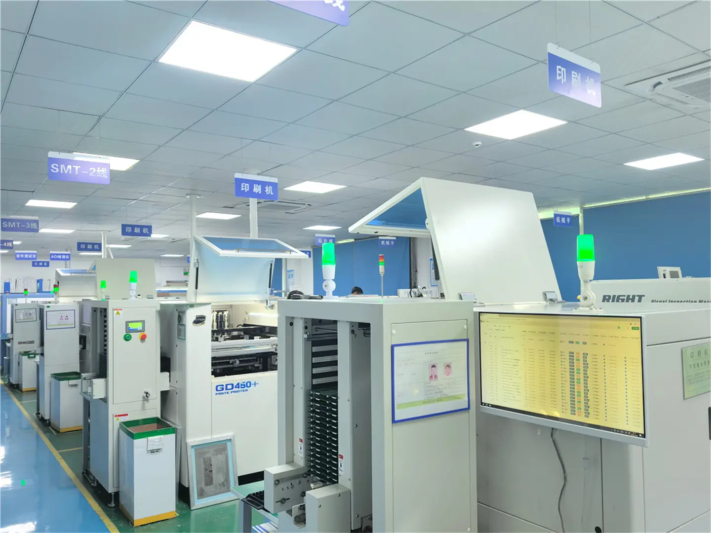
Millimeter-Wave Automotive Radar & Telematics Optimization
77–81 GHz automotive millimeter-wave radar modules require ultra-tight reflection controls to maintain target angular resolution and noise floor margins. Aozite engineers utilize high-frequency cavity back-drilling, Rogers-FR4 hybrid bonding, and precision automated solder paste height validation to eliminate radar blind-zone reflections.
Tolerance:±5% Controlled Z0
Inspection:3D X-Ray Voiding <10%
Traceability:Full Lot Serialization

High-Bandwidth Medical Diagnostic & Imaging Sensors
Diagnostic MRI, ultrasound transceivers, and digital pathology scanners rely on clean, unattenuated signal paths. Our return loss optimization controls stub resonances, via transitions, and micro-coaxial board launches, drastically decreasing phantom artifacts and signal degradation in ultra-sensitive patient diagnostics.
Testing:100% Vector FCT
Cleanliness:Controlled Ionic Residue
Standard:ISO 13485 Compliance
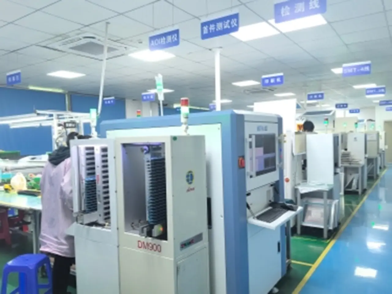
High-Speed Industrial Fieldbus & High-Current Control
Industrial automation networks running high-speed Industrial Ethernet (TSN, EtherCAT) often encounter severe signal degradation when routed near high-voltage motor drivers. We implement differential impedance matching, coplanar shielding, and automated conformal coating to prevent electromagnetic reflection under harsh factory noise.
Assembly:Mixed SMT & Wave DIP
Protection:Polyurethane / Silicone
Testing:Thermal Burn-in Aging
Engineering Execution
Closed-Loop Manufacturing & Testing Workflow
Every PCBA lot is subjected to an unbroken chain of precision verification from incoming substrate testing to Vector Network Analyzer (VNA) functional validation.
STEP 01
Incoming Material QC
TDR verification of raw copper foils, dielectric prepreg checking, vacuum component baking, and serialization.
STEP 02
3D Solder Paste SPI
Measurement of 100% aperture volume, height, and area offset to eliminate RF launch pad impedance deviations.
STEP 03
High-Speed Placement
Mounting of passives down to 0201/01005 alongside ultra-fine pitch BGAs with ±15μm robotic placement accuracy.
STEP 04
Nitrogen Reflow Solder
Custom multi-zone thermal profiling under N2 purge to mitigate oxidation and guarantee planar micro-soldering fillets.
STEP 05
In-line 3D AOI & AXI
Automated optical joint topology evaluation plus 3D X-Ray inspection of hidden ground vias and BGA voids.
STEP 06
Precision DIP & RF Launch
Selective soldering of high-frequency SMA/SMP edge launches and wave soldering for ruggedized power interfaces.
STEP 07
VNA S-Parameter FCT
Direct testing of return loss (S11), insertion loss (S21), and eye-diagram jitter according to custom firmware scripts.
STEP 08
Box Build & Packaging
Precision CNC housing integration, EMI gasket assembly, and hermetic anti-static packaging for global export dispatch.
Strategic Horizons
Return Loss Engineering: 2026-2030 Roadmap
As data rates scale past 224 Gbps PAM4 and terrestrial communications pivot into sub-THz satellite domains, impedance matching shifts from reactive correction to predictive materials synthesis.
PHASE 01 // 2026
Co-Packaged Optics (CPO)
Elimination of standard copper board traces via direct fiber termination on multi-chip packages, driving S11 reflection boundaries below -30 dB at 112G per lane.
PHASE 02 // 2027
AI-Assisted Stencil Metrology
Machine learning models dynamically adjusting micro-aperture laser cutting to counterbalance localized copper thickness variations and micro-strip fringing capacitance.
PHASE 03 // 2028
Sub-THz Substrate Integration
Ultra-smooth copper deposition on modified polyimide (MPI) and liquid crystal polymer (LCP) substrates suited for non-terrestrial satellite communication links up to 140 GHz.
PHASE 04 // 2030
Autonomous In-Situ TDR Tuning
Real-time automated board laser-trimming and embedded passive tuning performed directly during inline automated testing to correct individual component tolerance stackups.
Technical Clarifications
Frequently Asked Questions
Engineering insights into return loss optimization, impedance tolerances, factory quality control, and international turnkey collaboration.
What files and data parameters are required to evaluate an RF Return Loss Optimization project?
For comprehensive signal integrity optimization, our engineering team requires:
1. Complete Gerber files (RS-274X) or preferably ODB++ containing explicit layer stackup information and copper weights.
2. Bill of Materials (BOM) including precise manufacturer part numbers (MPNs), dielectric tolerance ratings, and alternate suggestions.
3. Pick-and-place centroid files along with specific high-frequency component datasheets.
4. RF specifications: Target characteristic impedance (Z0 ±% tolerance), frequency bandwidth of interest, target return loss (S11 in dB), and dielectric constant (εr) constraints.
5. Detailed functional circuit test (FCT) protocols, firmware images, and RF test fixture calibration parameters (such as TRL de-embedding data).
How does return loss differ from VSWR, and what constitutes an acceptable baseline?
Both metrics describe impedance matching efficiency:
• Return Loss (RL): Expressed in decibels (dB), representing the logarithmic ratio of reflected power to incident power (RL = -20 log|Γ|). A higher absolute positive value or more negative S11 indicates better matching.
• VSWR (Voltage Standing Wave Ratio): Represents the numerical ratio of maximum standing wave voltage to minimum voltage (ranging from 1.0:1 upwards).
In high-reliability industrial communications, a return loss of ≥ 20 dB (VSWR ≤ 1.22:1) denotes high performance (≤ 1% reflected power), while for standard consumer digital channels, ≥ 14 dB (VSWR ≤ 1.5:1) is commonly acceptable. Our Shenzhen optimization services frequently target ≤ -25 dB across mission-critical RF bands.
How do you handle prototype prototyping versus high-volume production pricing?
Our 8 high-speed SMT lines utilize the exact same precision pick-and-place setups and 3D SPI/AOI calibration processes for low-volume engineering prototype batches as they do for runs of hundreds of thousands of boards. While prototype runs reflect fixed tooling costs (precision laser stencils, line setup, feeder allocation, and minimum component reel packaging), our DFM engineers review your panelization layout and recommend alternate components to ensure prototype-level investments seamlessly scale into competitive volume manufacturing costs.
What closed-loop quality control mechanisms prevent RF degradation on the line?
We apply an integrated, audit-ready quality loop:
1. Incoming Inspection: Substrate dielectric verification and moisture barrier checking (MSD baking).
2. 3D Solder Paste Inspection (SPI): Real-time volume and height monitoring to avoid parasitic capacitance shifts on sensitive RF pads.
3. Post-Reflow 3D AOI: Automated alignment and fillet quality verification conforming to IPC-A-610 Class 2 standard (Class 3 on request).
4. 3D AXI (X-Ray): Quantitative void detection beneath bottom-terminated components (QFN/BGA) targeted under <10% voiding.
5. First-Pass Yield Target: Our operational metrics strictly target and achieve ≥ 98.5% first-pass yield across volume runs.
Can overseas buyers conduct factory audits or verify lot traceability remotely?
Yes. Overseas clients are invited to visit our Shenzhen manufacturing headquarters in person or book a live, guided video audit. During a video audit, our quality assurance directors take you through our raw material storage, cleanroom feeder setup, 8 automated SMT lines, X-ray testing station, and ERP batch tracking database. Every shipment includes comprehensive inspection reports, certificate of conformance (CoC), and full barcode-traceable lot documentation.
Comprehensive Assembly Portfolio
High-Reliability PCBA Manufacturing Services
Explore our full spectrum of IoT, industrial control, smart wearable, and bespoke turnkey manufacturing capabilities produced in Shenzhen.

Custom High-quality PCBA Assembly for IoT Control Boards
View IoT Control Boards →
High-Quality Industrial Control PCBA Assembly & Processing
View Industrial PCBA →
ODM One-stop PCBA Manufacturing & PCB Assembly
Explore Turnkey Assembly →
High-Quality OEM ODM PCBA for All Electronic Products
OEM/ODM Electronics →
ODM Earphone Panel PCBA OEM ODM Service
Audio Hardware Service →
OEM Smart Bracelet PCBA OEM Manufacturing
Wearable PCB Assembly →
OEM Professional SMT PCBA Production for Electronics
Advanced SMT Factory →