
Precision PCBA Solutions: Top OEM / ODM Deployments
Direct from our Shenzhen SMT facility: Explore our precision PCBA assemblies engineered to meet demanding thermal, RF, and miniaturized operational parameters.








Navigating Modern Electronics Procurement: Reliability Over Mere Cost
The global printed circuit board assembly (PCBA) sector is currently witnessing a massive transformation driven by edge computing, high-frequency 5G/6G RF nodes, high-voltage e-mobility systems, and IoT miniaturization. In modern high-reliability applications, procuring circuit boards cannot be treated as a commoditized transactional purchase. A subtle flaw—such as an unnoticed micro-void beneath an ultra-fine pitch Ball Grid Array (BGA), flux contamination beneath passive 01005 packages, or an untracked batch of degraded MOSFETs—can lead to catastrophic field failures, expensive warranty recalls, and irreversible brand damage.
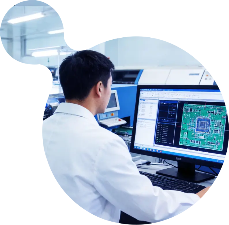
As international hardware developers and Original Equipment Manufacturers (OEMs) demand shorter innovation cycles, the role of a modern PCBA factory has transitioned from a basic "board-stuffing shop" into an integrated engineering partner. Factories must implement rigorous Design for Manufacturability (DFM), strict ESD safeguards, automated in-line optical inspection (3D AOI), 3D Solder Paste Inspection (SPI), high-resolution X-ray detection, and full-spectrum functional validation.
China's PCBA Supply Ecosystem: The Strategic Agility of Shenzhen
Shenzhen represents the apex of global electronics industrial clustering. Understanding this operational ecosystem clarifies why leading overseas OEMs maintain primary manufacturing hubs in this region.
Same-Day Sourcing Velocity
Situated within Longgang District, our factory operates inside Asia's densest component ecosystem. Passive reels, specialty microcontrollers, RF modules, and custom heat sinks can be sourced from verified tier-one franchise distributors within hours rather than weeks.
- Immediate access to franchise authorized channels
- Real-time verification against counterfeit components
- Same-day prototyping turnarounds for urgent engineering builds
Full Vertical Hardware Integration
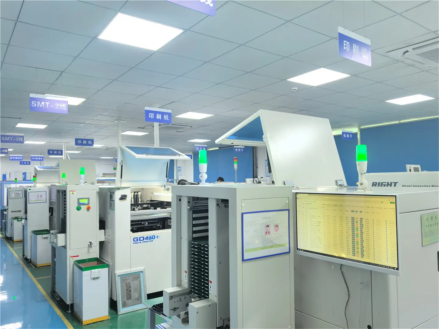
Rather than managing segregated bare-board fabricators, passives vendors, DIP insertion workshops, and boxing houses, our Shenzhen facility integrates every tier under a unified Enterprise Resource Planning (ERP) and Manufacturing Execution System (MES).
- Bare PCB fabrication with controlled impedance matching
- Precision laser cut electropolished stencils
- Automated conformal coating & custom enclosure box build
Engineering Risk Amortization
Our senior engineering directors, backed by over 20 years in high-density SMT operations, execute exhaustive DFM reviews before stencils are cut. We identify footprint mismatches, solder bridging risks, and thermal relief anomalies directly on Gerber/ODB++ files.
- Early obsolescence flagging & drop-in alternate parts
- Optimized reflow thermal profiling for lead-free SAC305
- Dedicated NPI (New Product Introduction) engineering cells
Localized Engineering Use Cases & Custom Board Applications
From industrial shop floors in Germany to smart home ecosystems across North America, our PCBA assemblies are purpose-engineered for challenging operational environments.
Harsh-Environment Vehicle Control & BMS Systems
Automotive electronics require superior thermal shock resistance, rigorous anti-vibration stability, and absolute defect-free operation. We assemble Battery Management Systems (BMS), On-Board Chargers (OBC), and in-cabin telematics adhering to IPC-A-610 Class 3 specifications. We utilize nitrogen-purged reflow ovens, automated underfill dispensing, and conformal silicone coating to eliminate condensation risks and solder cracking.
- Inspection: 100% 3D X-Ray verification ensuring BGA void rates remain strictly under 10%.
- Reliability: Thermal cycling testing from -40°C to +125°C to confirm joint integrity.

Zero-Tolerance Healthcare & Patient Telemetry Devices
Medical hardware demands unwavering repeatability, low ion residue levels, and absolute traceability down to individual component reels. Our cleanroom assembly processes support patient monitoring terminals, IVD analyzers, and wearable health patches. Assemblies are produced using clean-flux chemistries and validated via automated ionic contamination testing.
- Traceability: Full lot serialization tying each barcode to specific SMT feeder lines and reflow logs.
- FCT Testing: Custom bed-of-nails functional fixtures executing firmware flashing and sensor validation.
Continuous 24/7 Operations: PLCs, Inverters & Wireless IoT
Industrial machinery cannot afford unexpected downtime. We manufacture mixed-technology PCB assemblies combining fine-pitch microcontrollers with heavy through-hole DIP connectors, power inductors, and terminal blocks. Wave soldering is tightly managed with titanium pallets to protect sensitive surface-mount devices on dual-sided assemblies.
- Protection: High-dielectric conformal potting resistant to oil mist, dust, and corrosive gases.
- Burn-In: Optional elevated-temperature burn-in chambers to filter out infant mortality failures.
PCBA Engineering Roadmap: Pioneering AI-Driven SMT & Advanced Packaging
As microelectronics shrink and edge AI hardware proliferates, manufacturing tolerances leave zero margin for error. Discover our technological progression roadmap designed to support next-generation hardware designs.
High-Density Interconnect (HDI) & 01005 Micro-SMT
Standardized placement capability down to 01005 (0402 metric) passives and 0.35mm pitch CSP/BGA components. In-line closed-loop 3D SPI dynamically communicating with Yamaha and Panasonic pick-and-place systems to continuously auto-correct stencil offsets.
AI-Powered Automated Optical & Defect Classification
Integration of deep-learning convolutional neural networks (CNN) into 3D AOI inspection stations. This eliminates false calls caused by PCB surface reflectivity, increases detection speeds by 40%, and pinpoints micro-solder bridging beneath low-clearance ICs.
Embedded Components & SiP (System-in-Package) Assembly
Expanding capabilities in sub-board cavity assembly, rigid-flex multi-layer stack-ups, and embedded passive substrate manufacturing. Specially optimized for medical wearables, defense RF terminals, and ultra-miniaturized consumer audio designs.
Low-Temperature Soldering (LTS) & Carbon Neutrality
Validating Bi-Sn-Ag low-temperature solder alloy profiles to reduce peak reflow oven thermal exposure from 245°C to 170°C. This eliminates thermal stress on thin substrates, reduces warpage, and cuts manufacturing carbon footprint by up to 28%.
Global Certification, Traceability & Multilingual Support
Overseas buyers require more than low quotes; they require institutional trust, airtight legal compliance, and clear communication across international time zones.
Full Process Certifications
Our workshop processes strictly adhere to IPC-A-610 Class 2 standard (Class 3 on demand) and J-STD-001 soldering criteria. All assemblies fully comply with international RoHS, REACH, and UL flammability (94V-0) environmental standards.
Complete Batch Audit Trail
We provide full material certs (CoC), mill test certificates for substrates, solder paste melt analysis logs, and comprehensive functional test logs. Auditing teams can review line operations via live high-definition video feeds or on-site inspections.
Dedicated International Desk
Direct communication with fluent, technically proficient bilingual project managers. From Initial BOM scrubbing and DFM query reports to door-to-door DDP air/sea logistics coordination, our response window is guaranteed under 2 hours during active business hours.
Frequently Asked Questions: Sourcing Custom PCBA Factories
In-depth technical answers addressing quoting parameters, component integrity, quality gates, and IP protection for international engineering teams.
What engineering documentation is required for an authoritative turnkey PCBA quote?
- Gerber or ODB++ Files: Including all copper routing layers, soldermask, silkscreen, drill files, and mechanical edge cuts.
- Complete Bill of Materials (BOM): Formatted with exact manufacturer part numbers (MPN), approved second-source equivalents, reference designators, package footprints, and part descriptions.
- Pick-and-Place (Centroid) Data: Containing X-Y coordinates, board side (Top/Bottom), and component rotation angles.
- Assembly Drawings & Testing Specifications: Highlighting critical connectors, sensitive components, keep-out zones, firmware flashing binaries, test point voltages, and functional criteria.
How does your factory protect against counterfeit or substandard electronic components?
What is your standard protocol for NPI (New Product Introduction) and prototypes?
Can overseas buyers execute an on-site or digital factory audit before issuing a PO?
How do you ensure intellectual property (IP) and firmware confidentiality?
High-Reliability PCBA Manufacturing Catalog
Explore additional proven electronic manufacturing builds. Select an assembly series to review full engineering specifications, fabrication layers, and turnkey capabilities.